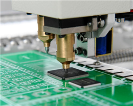
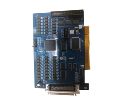
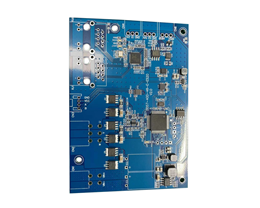
For SMT chip processing, solder joint voids are a serious quality problem. The presence of voids will increase the oxidation of the product, leading to the deepening of the aging reaction of the product in advance. So, how do the hollows in SMT chip processing occur? Let the Shenzhen PCB manufacturer explain it for you in detail below:
1. The cause of solder paste. The alloy composition of the solder paste is different, and the size of the particles is different, which will cause bubbles during the solder paste printing process, and some air will continue to remain during reflow soldering, and voids will be generated after the bubbles burst at high temperatures.
2. Surface treatment of PCB pads. The surface treatment of the pad also has a crucial effect on the generation of voids.
3. Reflux curve setting. If the reflow soldering temperature rises too slowly or cools down too fast, the residual air inside cannot be effectively eliminated, resulting in voids.
4. Backflow environment. Whether the equipment is vacuum reflow soldering also affects the generation of voids.
5. Pad design. The unreasonable pad design is also a very important reason for voids.
6. Micropores. This is a point that is easily overlooked. If the micro-holes are not reserved or the positions of the micro-holes are not correct, voids may occur.