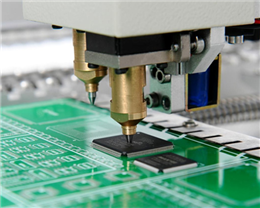
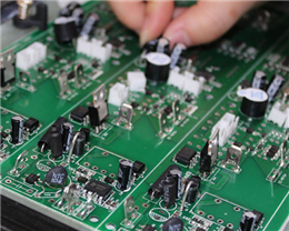
As a professional pcba proofing platform, we often encounter incomplete information provided by many customers, resulting in delays in delivery. In order to save time and improve consumption efficiency, the editor of Kuaifa Zhizhi will share today: the demand for proofing in smt What information is provided?
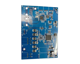
Gerber data file: If you choose the smt patch processing plant to stop the placement, you need the Pad layer, solder mask layer, silk screen layer, and stencil layer in the Gerber data when opening the stencil and manufacturing the patch process; if only smt is required When the assembly plant suspends the OEM business, it only needs to provide the documents required by the processing plant of the smt OEM; if your board is a jigsaw, you need to provide the jigsaw file.
BOM: It is the bill of materials. When the smt patch proofing is stopped, the material list required by theory is included. The information must be detailed and accurate. If there is any change, it should be noted on the BOM.
Coordinate file: It is required to provide the origin of the PCB board for smt patch processing, which is usually placed in the lower left corner of the design, and the location information of the components needs to be drawn. The extension is required to be in .txt or Excel format; the unit is metric, and mm (millimeters) is used by default. .
Location map file: The pad and silk screen layer of the PCB file exported from the R&D software, smt placement is used to check whether the placement of the SMT material is correct.
Test guidance documents: guidance and technical requirements for professional parameters in testing.